Twin Creeks Technologies' CEO Siva Sivaram spoke in wildly aspirational terms about the firm's ion-implant machine and the ability to produce super-thin photovoltaic cells from crystalline silicon in the company's public debut earlier this year.
Today the company sold its assets for approximately $10 million to GT Advanced Technologies (Nasdaq: GTAT), according to the GT website. The firm had raised more than $80 million from Crosslink Capital, Benchmark Capital, Artis, and DAG Ventures. The deal also includes royalties from future sales.
GT will pursue substrates for power semiconductors, solar wafers, and thin sapphire laminates for touch screens with the ion-implant equipment.
As for Twin Creeks, the firm picked a bad time to enter a ruthless solar market. Today's over-capacity solar industry is not hungry for innovation or capital expense -- and Twin Creeks was heavy on both.
GT aims for commercialization of the technology in late 2014. The good news is that the innovative work at Twin Creeks lives on at GT.
Sivaram wrote in an email that "about 20 people in Boston are part of the transfer" and also emitted the obligatory phrase: "The management of Twin Creeks supported the private sale and feels confident that GT is in an excellent position to commercialize this innovative technology."
Here is some background on the Twin Creeks technology:
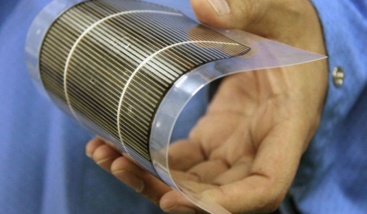
Twin Creeks Technologies looks to help solar module makers reduce the amount of silicon used -- by allowing them to make extremely thin solar cells. (Silicon accounts for about 20 percent to 25 percent of the cost of a PV module.)
Current silicon wafer thickness is in the 150-micron range. Traditionally, wafers are freed from blocks of silicon using wire saws in a process that is messy, complex and reaching its limits. It's an obvious weak link and cost target in the solar value chain. Manufacturers spend a great deal of time and energy to fabricate blocks of polysilicon, only to see up to half of that hard-earned material turned into sawdust in the wafer production step.
In fact, according to Twin Creek's CEO Siva Sivaram, you only need wafers that are 20 to 30 microns thick to get the charge carrier out while still getting good conversion efficiencies.
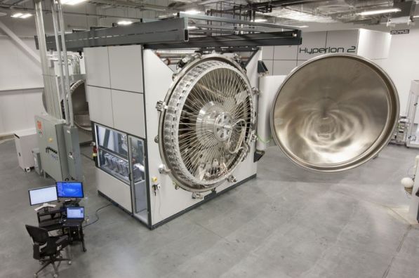
Twin Creeks allows vendors to dispense with saws, furnaces, and cell finishing equipment from the likes of Applied Materials HCT and Meyer Burger as well as slurry and thick wafers. Twin Creeks replaces that production chain with a beast of an ion implant machine (see picture below).
Ion Implantation
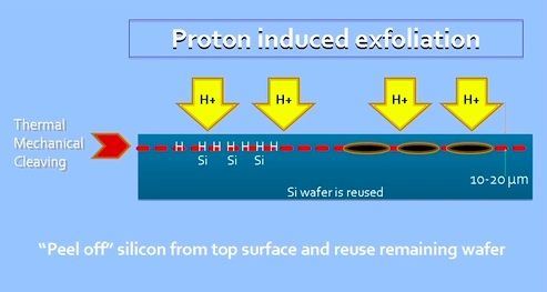
Twin Creek's process is known as Proton-Induced Exfoliation (or PIE). A hydrogen ion or proton is accelerated to 1.2 million electron-volts and shot into a crystal material -- in this case, silicon -- where it settles at a finite depth. The hydrogen ions line up at that finite depth, where they are then heated, resulting in a wafer that cleaves right off the substrate along the crystalline plane.
The proton energy determines how deep the protons go and therefore sets the thickness of the wafer.
An ion implanter is a big piece of equipment emitting protons and must be shielded for safety. Other firms performing this process have told GTM that surface roughness is better than sawn wafers, and some use an etch-and-anneal step to preserve lifetime once the wafers are cleaved.
The ion-implant process produces a wafer which uses a tenth of the material, and 20-micron wafers don't crack, according to the Twin Creeks CEO, who said, "At 20 microns, silicon is completely flexible."


 41
41
 15
15
 9
9