In 2013, 1366 Technologies of Bedford, Mass., a startup with VC funding and a DOE loan guarantee, opened a $6 million, 25-megawatt wafer fabrication facility. Today, the company announced plans to build a 250-megawatt commercial solar wafer manufacturing facility in Genesee County, New York.
The intention is to eventually scale that factory to 3 gigawatts of cell capacity and hundreds of millions of wafers per year. This makes 1366 Technologies the "anchor tenant" at the Science and Technology Advanced Manufacturing Park in New York’s Finger Lakes region. And with SolarCity's gigawatt-scale solar factory not too far away, New York state is now positioned to be the leading solar cell producer in the country.
It's taken a while for 1366 to get to this point. Frank van Mierlo, the CEO of 1366, said in a statement, "We’ve taken a very deliberate route to high-volume production. In the process, we’ve built a stable, capital-efficient business during the most challenging of times.” He also said, "the facility in Bedford, Massachusetts was our proving ground" and "New York brings us to commercial scale."
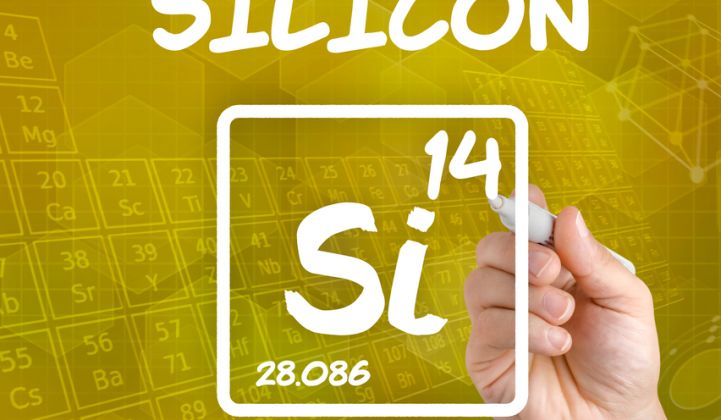
The company's technology falls in the kerfless wafer category, a technology that was of special interest to former DOE head Steven Chu. 1366's technology creates wafers directly from molten silicon, though the firm has not divulged specific details about its process. Other companies in the kerfless silicon sector include Solexel and Crystal Solar.
The aim is to disrupt the traditional way that silicon-based photovoltaic wafers are fabricated. The company claims that it has demonstrated "manufacturing rates of more than 1,200 wafers per furnace per day -- with a goal of more than 3,500 wafers per day for each furnace -- on par with standard ingot casting furnaces."
As van Mierlo told GTM in a previous interview, "For the last 50 years, we've been melting silicon, creating ingots and blocks, and cutting the blocks with wire saws to create wafers," adding that the incumbent process uses 18 different machines and goes through "a lot of consumables." He continued, "Half of the silicon is wasted. Our process has none of these consumables," said the CEO, noting that 1366 uses one-quarter of the factory real estate and doesn't waste silicon in its "semi-continuous process."
The end product is a textured wafer in a standard 156-by-156-by-0.2 millimeter size. According to the CEO, "It goes into any standard cell line." The process has yielded efficiencies of 17.2 percent in customer trials, according to the company. “1366 Technologies has the enormous benefit of being a ‘drop-in’ replacement for 60 percent of the photovoltaics market,” said Hidenori Okamoto, managing executive officer of Tokuyama Corporation, an investor in 1366.
The company claims that the factory will be "strategically located" between the New York cities of Rochester and Buffalo.
On top of the incentive of the balmy Mediterranean weather the region is known for, a release notes, "To encourage 1366 Technologies to invest and establish operations in New York, Governor Cuomo’s administration offered a competitive and attractive incentive package through various state and local resources including Empire State Development, New York’s chief economic development agency; New York State Energy Research and Development Authority (NYSERDA); New York State Homes and Community Renewal; New York Power Authority; and Genesee County Industrial Development Agency.
The New York state contribution to this endeavor will be about $97 million, according to the governor, who was in attendance at the site today.
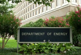
The company's total equity financing is $69.5 million from investors including Tokuyama Corporation, North Bridge Venture Partners, Polaris Venture Partners, VantagePoint Capital Partners and Energy Technology Ventures (a JV involving General Electric, NRG Energy and ConocoPhillips), Hanwha Chemical, Ventizz Capital and Haiyin Capital. In addition, 1366 has won several million dollars in DOE grants, as well as a $150 million loan guarantee offer from the DOE's 1705 program, which will be drawn down for the build-out of this factory.
Construction of the 130,000 square-foot facility is expected to be completed in 2017.
Van Mierlo has likened the 1366 innovation in silicon to the Bessemer process innovation at U.S. Steel or the use of float glass at Pilkington. He notes that the Bessemer process was the result of a decades-long innovation path.


 41
41
 15
15
 9
9