Realizing that science is approaching the limits of standard solar cell efficiency, Caltech physicists decided to shift the research focus from the cell’s active material to its coating.
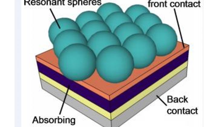
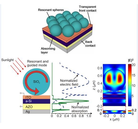
Using the phenomenon of Whispering Gallery Modes, which describe the way whispers under cathedral-like domes can be clearly heard far across the room, the physicists designed a commonplace, inexpensive coating that theoretically increases by twelve percent to fifteen percent the light delivered to a typical thin-film amorphous-silicon (a-Si) solar cell’s photovoltaic (PV) material. If it works, it could be a boost for amorphous, which trails other PV materials in efficiency.
Some of the world’s smartest material scientists have thought long and hard about silicon and other photovoltaic materials like cadmium telluride (CdTe) and cadmium indium gallium diselenide (CIGS), which release electrons when hit by light. In recent years, they have struggled to increase solar cell efficiencies by even one percent.
Caltech physicists in Harry Atwater’s Applied Physics laboratory decided to approach the question of efficiency from a different point of view, as described in "Light Absorption Enhancement in Thin-Film Solar Cells Using Whispering Gallery Modes in Dielectric Nanospheres" by Jonathan Grandidier, Dennis M. Callahan, Jeremy N. Munday, and Harry A. Atwater.
“There are a lot of people in material science that are studying different types of materials like amorphous silicon or gallium arsenide,” Caltech post-doctoral fellow Jonathan Grandidier said. “This is a whole science by itself.”
“What we tried to demonstrate is that by starting with any thin-film solar cell with smooth surfaces and fabricated on a flat substrate,” Harry Atwater further explained by email, “we could enhance the absorption by applying a coating to the thin film cell, without roughening the flat, smooth surfaces.”
Though their concept involves a layer of nanospheres arrayed above the PV material, it is “a really different project” from the previously published Caltech work with nanowires grown on the surface of PV material to enhance the light-absorbing area. “Our starting point is a finished, perfectly flat solar cell,” Grandidier explained.
“The idea was to catch the light inside the spheres,” said Grandidier. “This light, this energy, inside the spheres could be absorbed into the solar cell, which is under it.”
The more light that hits the PV material in the cell, the more electrons are released and the more electricity is generated. By layering silicon dioxide (silica) spheres over any PV material, the amount of light that is captured and transferred can be increased. Similarly, Innovalight has boosted crystalline silicon solar cell performance through added layers.
“By tuning the size of the sphere, you can vary the position of the resonance,” Grandidier said. Varying the resonance improves the capture and transfer of different levels and angles of light, increasing solar cell efficiency as light conditions and the sun’s position in the sky change. These changes can be made “not only by tuning the size but also by tuning the spacing,” Grandidier said. “But tuning the spacing is a little bit trickier.”
The physicists’ paper, just accepted as the October 2011 cover story for the scientific journal Advanced Materials, is based on “completely theoretical” results, Grandidier said. Its conclusions are the result of “doing numerical simulations” of how light would affect “a nanosphere array above a typical thin-film amorphous silicon solar cell structure with a back contact of silver and a transparent ITO film contact conductive layer.”
“The experimental part is in progress,” Grandidier explained.
Fabrication of the hypothesized solar thin film necessitates depositing the nanosphere array, Grandidier said, which “adds another step to the cell fabrication process.” But researchers examining the problem of depositing nanospheres on a flat surface have developed a method and Grandidier does not expect the deposition of the nanosphere array to add significantly to the cell fabrication process, though he admitted that remains to be seen.
The most exciting aspects of the research are that (1) the nanosphere array layer is calculated to produce a twelve percent to fifteen percent increase in sunlight absorption of typical anti-reflection coated a-Si thin film solar cells, (2) the array can be made from common and cheap silicon dioxide or polystyrene, and (3) known and existing manufacturing processes can be used to add it to typical thin-film solar cells.
“There are no commercial plans at this point,” Grandidier said. The researchers expect further experimental work to clarify ways that spheres of different sizes can be used to tune both size and spacing for even more optimum efficiencies. They will also be studying how “to maintain spheres together in the long term and to protect them against usage,” according to Grandidier.
"The ability to engineer the photonic environment of a solar cell,” Callahan wrote in an email, “is basically a brand new degree of freedom.” He added that “solar cells of the future will most likely have some degree of photonic engineering” and that this concept’s “low cost, low loss, scalable” proposal “may give it a natural advantage.”


 41
41
 15
15
 9
9