Below is analysis from GTM Research report author Andrew Gabor. For more information on the technologies discussed, see Innovations in Crystalline Silicon PV 2013: Markets, Strategies and Leaders in Nine Technology Areas.
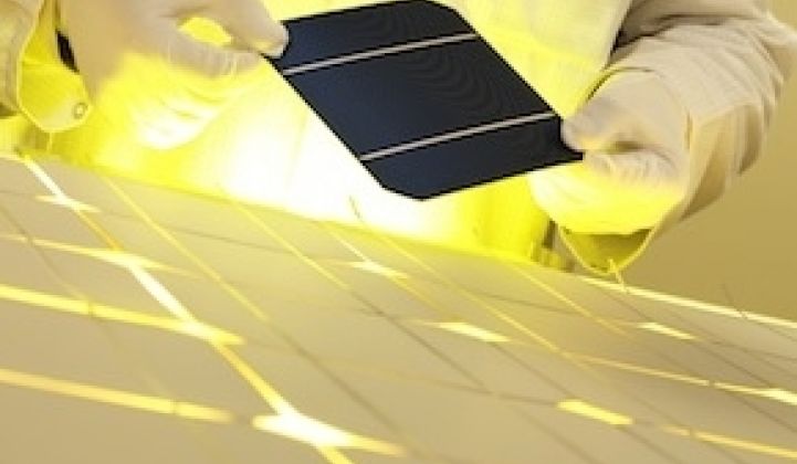
Has the trend toward thinner solar cells ended? It seems like the industry has paused at the 180- to 200-micron-thick wafer level.
With the dramatic plunge in polysilicon feedstock prices, the motivation to go thinner may not be worth the hassle for manufacturers; this is due to the problems of increased yield loss from breakage, difficulties with handling and processing bowed cells after metallization firing, and an increased percentage of cracked cells within modules, which may translate to lower nameplate power ratings and worse degradation rates in the field.
Still, savings on the order of $0.10 per wafer or more are possible from thinning down the wafers, particularly if module performance can be maintained or actually improved. Briefly described below are ten technologies that can help enable thinner solar cells, listed roughly in order of the ease of implementation.
- Low-bow aluminum pastes: As usual, metallization pastes lead the list in enabling technological progress within the PV industry. All of the major paste vendors are working on aluminum paste variations that cause less bowing of thin cells.
- Diamond wire sawing: This wafering method is used primarily for monocrystalline ingots, but several companies are also exploring its use for multicrystalline ingots where wire breakage costs tend to be higher. In contrast to the standard SiC-slurry wire sawing approach, the fixed abrasive in the more expensive diamond wire allows for not only much higher cutting speeds, but also for lower total thickness variation across the wafer area. This reduction in thickness variation can ease the transition to thinner wafers.
- Conductive adhesives: Why do cells crack after soldering? The culprit is largely the flat copper wires that interconnect the cells. When cooling from the soldering operation, the stress from the differential contraction between the copper (high expansion coefficient) and the silicon (low expansion) creates microcracks under the wires in the silicon. These microcracks can propagate into full cracks more easily when the wafers are thin. By bonding the wires with conductive adhesives instead, the stress and microcrack formation are largely eliminated. Common concerns with conductive adhesives are cost and reliability. The graph below shows how by eliminating the front silver-paste busbars and bonding wires directly to the fingers with standard silver-filled conductive adhesives, the costs can actually go down. Other benefits from this approach add to the potential cost savings and module design freedom. Concerns about galvanic corrosion at silver/tin interfaces can be addressed through use of Dexerials' and Hitachi Chemicals' conductive tape materials that are used already at high volume in Panasonic’s HIT modules. Hitachi Chemicals’ hybrid CP-300 material with epoxy and solder characteristics is also promising. Thus, conductive adhesives can lower costs, enable thinner wafers, improve efficiency, and improve module reliability.
FIGURE: Calculation of Cost Component Increases and Decreases for Conductive Adhesive Stringing vs. Standard Stringing
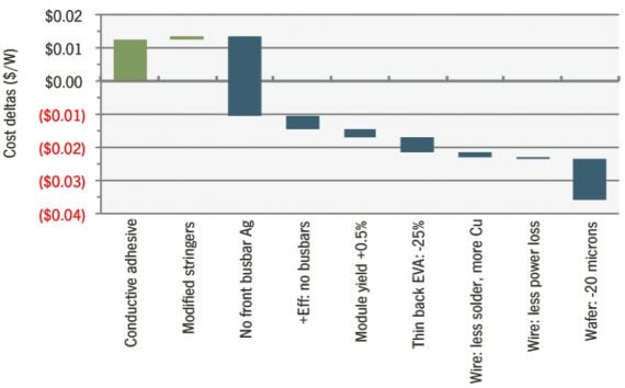
Source: Innovations in Crystalline Silicon PV 2013: Markets, Strategies and Leaders in Nine Technology Areas
- Rectangular cells: By using half-size cells, the bowing problem is reduced. In addition, the resistive power losses in the interconnect wires are greatly reduced since these scale as the square of the current. This frees up the design space to allow the use of thinner wires, which cause fewer microcracks. Mitsubishi Electric and other companies are pursuing this approach. The downside is of course increased capital expenditure for some handling and processing steps, depending at which point in the process the cells are cut.
- Interconnect wire arrays: In this approach, the two or three flat interconnect wires are replaced by an array of twelve or more round wires. Invented by Day4 Energy, variations on this approach are being commercialized by equipment vendors Meyer Burger and Schmid. The Schmid variation still uses solder, but the stresses and microcrack distributions are likely different so that crack propagation may be less common. In either case, due to the larger number of redundant current paths, the modules are much more tolerant to cracks.
- Rear Dielectric Passivation: By placing a patterned dielectric layer between the rear aluminum paste and the wafer, the paste will cause less bowing of the thin cells. Cell efficiency can also be improved, but the potential improvement is higher for monocrystalline wafers than for multicrystalline. Rear-side wet-etching/polishing (e.g., RENA, Schmid) that generally accompanies this approach also helps to strengthen the thin wafers. A variation on this approach uses physical vapor deposition of the aluminum layer for reduced materials costs, but higher capital expenditure.
- Metallization Wrap Through Cells: In this approach both the positive and negative contacts are placed on the back side of the cells. Rather than using interconnect wires, a patterned conductive backplane material may be used, although the costs associated with this can be high. The stresses associated with soldering at discrete points rather than continuous lines may be advantageous (or worse). Eliminating the front busbars improves cell efficiency, although processing costs are increased. Canadian Solar is one of the leading companies implementing this technology with its ELPS series of modules. In addition, this approach may also be combined with conductive adhesives.
- Interdigitated back contact cells: These SunPower-style cells have positive and negative contacts on the rear side along opposite edges so that only a short piece of interconnect ribbon is needed. Thus, soldering-induced damage is greatly reduced in SunPower cells, and this has enabled their industry-leading 135 micron wafer thickness. They also have no fired aluminum paste to cause bowing. Of course, the cost of manufacturing these cells is much higher.
- Kerfless wafers with a carrier: Solexel and Crystal Solar are examples of companies that exfoliate very thin, epitaxially-grown wafers from thick monocrystalline substrates. During the early stages of cell processing, these substrates act as a sturdy handle for the wafers to enable high mechanical yields. Later, after exfoliation, the cells are again securely bonded to another carrier (printed-circuit-board material or glass) for robust processing of the remaining steps. The carrier represents an additional material cost, but it also can add functionality and displace other costs. Solexel claims to have figured out a low-cost, interdigitated-back-contact cell design with this approach.
-
Standard wafers with a carrier: If the carrier approach works for the kerfless guys, why not try it for conventional wafers? Is anyone pursuing such an approach?
For more information on these technologies, see GTM Research's latest solar report, Innovations in Crystalline Silicon PV 2013: Markets, Strategies and Leaders in Nine Technology Areas.


 41
41
 15
15
 9
9