
Solexel, the former Soltaix, is still tight-lipped about their thin silicon solar activities.
But an article in Business Times released in Malaysia yesterday said that the company's CEO, Mike Wingert, is scouting out manufacturing sites in Malysia's Senai Hi-Tech Park. The article also said that Solexel is pledging to invest RM2.8 billion (that's $941 million) over five years to build a multi-gigawatt-capacity photovoltaic cell manufacturing plant. The company will be in the business of building solar modules, according to Ryan Brown, Director of Corporate Development at Solexel, in an otherwise non-informative phone interview.
That's a lot of money. And although the firm has raised funding from Kleiner Perkins, Technology Partners, DAG Ventures, The Westly Group, EcoFin, Spirox, Oakhill, Univest and Northgate Capital, they are probably a bit short of $941 million. The firm closed a $15 million A round in 2007, an undisclosed B round in 2008 and raised some additional funding from The Westly Group in 2010. The company looks to have more than 100 employees.
CEO Michael Wingert said construction "will start in 2012, and the plant will provide jobs for more than 2,300 people."
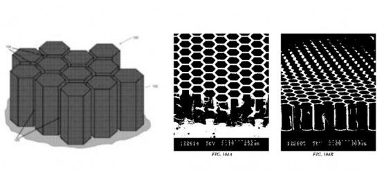
Judging by the NREL disclosures and patent information, Solexel is working on an epitaxial lift-off scheme using Porous-Silicon-Process (PSI process) technology licensed from the Max Planck Society, as well as some 3D wafer features including prisms and a "honeycomb" array.
Here's the patent for three-dimensional solar cells with honeycomb prisms. Here's a patent for manufacturing three-dimensional thin film silicon solar cells. And here's a patent for releasing a thin film substrate from a reusable semiconductor template. Here are links to some other Solexel patents. Most of the patents are invented by Mehrdad Moslehi, the founder and CTO of the firm.
Solexel received about $3 million in DOE incubator money in late 2008 with this description:
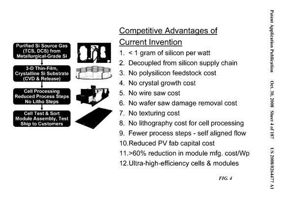
Solexel plans on commercializing a disruptive, 3D, high-efficiency mono-crystalline silicon cell technology, while dramatically reducing manufacturing cost per watt. At the end of this project, Solexel plans to deliver a 17-percent to 19-percent efficient, 156x156 mm2, single-crystal cell that consumes substantially less silicon per watt than conventionally sliced wafers.
When Solexel was formed, solar modules were selling in the neighborhood of $4.50 per watt. Today you can buy a reputable brand's module for $1.40 per watt; the price is far less if you're a large-scale developer. A CEO colleague told me he received a quote from a second tier vendor for $0.85 per watt. This is occurring at gigawatt-scale, and if this year so far is any indication, at increasingly slim margins.
This is the new solar landscape that Solexel is going to have to play in -- a landscape they might not have imagined when they first formed.
Here are some images from Solexel's patent filings:
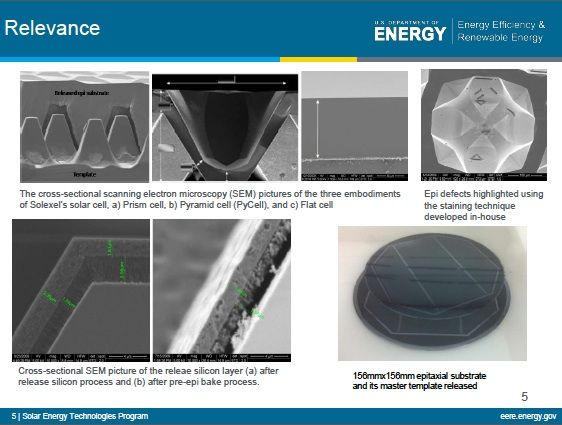
Here are some images from NREL presentations.
Other startups innovating in the thin silicon field include:
AstroWatt, as reported by Ed Gunther, has developed a Semiconductor-on-Metal technology for creating thin silicon wafers. Gunther reports, "After partial processing, a monocrystalline silicon wafer is attached to an inexpensive, flexible 50 um metal foil also acting as the solar cell’s rear contact. Next, the foil, along with about 25 um of silicon, is exfoliated using a cleaving process. By reusing a 600 um wafer for multiple exfoliations, AstroWatt claims that “up to 4X [four times] reduction in substrate cost” is possible, and the metal substrate is crucial for wafer handling in existing equipment. AstroWatt also stated the theoretical peak silicon solar cell efficiency can be achieved with a 25 um silicon wafer thickness. The company targets 20 percent efficiency while utilizing significantly less silicon.
Silicon Genesis, known as SiGen, promises kerf-free wafering via an implant-and-cleave process that is still in the early stages of development but could yield wafers with thicknesses down to 20 microns.
Ampulse claims that the firm’s "c-Si thin-film technology takes advantage of HW-CVD techniques to directly deposit a very thin layer of c-Si onto a uniquely textured and flexible metal substrate."
Bandgap Engineering has developed tunable methods for nano-structuring silicon. The firm claims that the absorption of nano-silicon is enhanced by up to several orders of magnitude over bare silicon over a wide range of wavelengths. This enables nano-silicon to absorb the light in the first four microns versus the top 50 to 100 microns that bulk silicon needs to absorb most of the light. This could impact cell efficiency and direct manufacturing cost -- and make for much thinner wafers.
Crystal Solar uses a vapor deposition process for making thin crystalline silicon wafers. The firm has made wafers measuring 50 microns thick in its labs and hopes to get down to 20 microns. Oceanshore Ventures is one of the firm's investors.
Twin Creeks Technologies is also working with ion implant technology, as per this patent.
1366 Technologies has a "direct wafer" technology where molten silicon is directly converted into wafers, which can then be processed into thin solar cells.
Others? Thin Silicon (looks more like a-Si), Clean Cell?


 41
41
 15
15
 9
9