I ran into the CTO of Massachusetts solar startup Bandgap Engineering at a Sierra Ventures-sponsored VC shindig in Menlo Park, CA and interrogated her over cocktails and crudites.
Marcie Black is an MIT and Los Alamos National Laboratory alum, now heading the technical team at the New Enterprise Associates, a (NEA) funded solar aspirant. Other investors include Sumitomo Corporation and the Massachusetts Green Energy Fund. Dr. Forest Baskett, General Partner at NEA is a board member. Bandgap closed a $6 million Round A-1 in June of 2009 and a $1.4 million round from those investors in 2008.
CTO Black's LinkedIn profile describes her work as a grad student at MIT, where she "investigated the optical absorption in bismuth nanowires and identified the main absorption mechanism as a particular electronic transition." She also threatens that she "can talk for hours about this if you are interested." Here are links to some of Black's related patent applications: Nano-structured optolectronic devices and devices with enhanced electronic transitions.
The firm has trademarked the term "nano-silicon" and the company website claims that they "can make [silicon] even better."
Bandgap has developed tunable methods for nano-structuring silicon. Unlike bulk silicon, nano-silicon's optical properties can be tuned to reduce reflection and increase absorption, critical characteristics for any solar cell.
The firm claims that the absorption of nano-silicon is enhanced by up to several orders of magnitude over bare silicon over a wide range of wavelengths. This enables nano-silicon to absorb the light in the first four microns versus the top 50 to 100 microns that bulk silicon needs to absorb most of the light. This could impact cell efficiency and direct manufacturing cost -- and make for much thinner wafers.
How thin? The CTO spoke of 20 micron dimensions -- which is pretty thin compared to the current PV wafer thicknesses in the 100-to-200-micron range. Although the CTO spoke of being in the wafer business, 20 microns may put the company into thin film or foil territory and the CTO did not rule out crystalline silicon thin films. (Ampulse, SiGen, and AstroWatt are also working in this dimensional realm as might be Twin Creeks Technologies. The Peumans group and the Cui group at Stanford are doing deep research on nanowires for photovoltaics and energy storage. Information on reciprocating dingle-arms here.)
Bandgap claims that solar photovoltaic cells based on nano-silicon have less reflection than bulk silicon or a traditional PV cell. Specifically, while bulk silicon reflects over 30 percent of light across the spectrum (at normal incidence) and PV manufacturers are able to reduce this to 5 to 8 percent with anti-reflective (AR) coatings and surface texturing, nano-silicon can reflect less than 1 percent of incoming light.
In most PV cell designs, thin metal lines are typically used as the front-side electrical contact. Because these metal lines shade the absorbing material below, they can block up to 5 percent of incident light from reaching the silicon. In contrast, Bandgap’s device design features a submerged front contact that is deposited in the same step as their nano-structuring. This can greatly reduce front side shading losses, according to the CTO.
The firm is not going to build modules (much to the joy of their VCs, I'm sure); instead, they are going to build cells. But the startup's value proposition is their process, which the CTO claims can improve efficiencies of PV cells by more than one percentage point. And that starts to sound a bit like Innovalight's (seemingly successful) business plan, which is more of a licensing or equipment play. Meanwhile, 1366 Technologies is also trying to bring new processes or equipment into the PV production line.
There is also some application for this technology in high energy density Li-ion batteries. Silicon is known to have high lithium absorption capacity, but it cannot be cycled due to “pulverization” during cycling. Bandgap and others have shown that a silicon architecture composed of aligned nanowires in a high-density "carpet" can achieve high energy density while remaining resistant to pulverization.
Is this the disruptive "new Black Swan improbable pyro-nano-quantum-thingamajig technology" that Vinod Khosla is looking for? Maybe not -- but incremental progress is a good thing, as well.
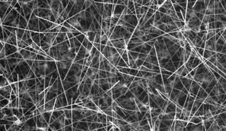
Picture of nanowires from Bandgap's website:


 41
41
 15
15
 9
9