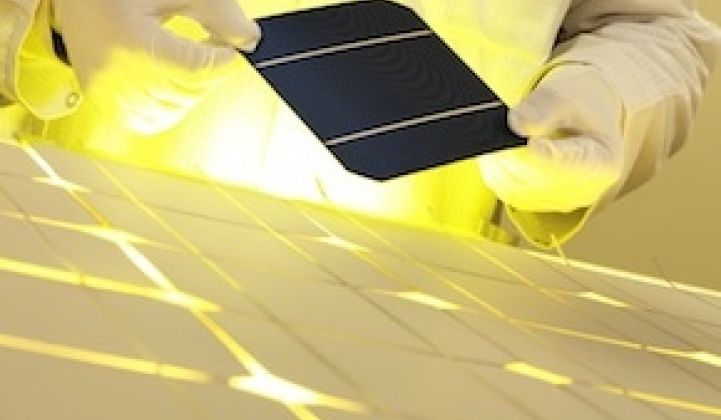
GTM Research’s latest report, titled Innovations in Crystalline Silicon 2013: Opportunities, Challenges, Costs and Leaders in Nine Technology Areas, is out today, and it’s a refreshing distraction amidst the gloom that hangs over an industry that has been bleeding money for the last year and a half. Authored by Andrew Gabor, formerly of Evergreen Solar and 1366 Technologies, the report takes a close look at several emerging technology areas in crystalline silicon technology that could alter the well-established process flow and device architecture of the c-Si value chain. Each of these concepts aims to improve some combination of factors that are essential to lowering installed or delivered costs of energy, be it cell/module efficiency, energy yield, material utilization, or manufacturing throughput. Below, we present a selection of key insights about the technology areas covered in the report.
Quasi-Mono/Cast Mono
“Has a solid two- to three-year run ahead of it, but … will face severe challenges after that point. In the long term, we see the bigger challenge to multi [crystalline] market share to be from reductions in the cost of CZ-mono wafers and from cell architectures that are dependent on CZ-mono-quality material.”
Diamond Wire Sawing
“While the cost benefits of using diamond wire may be small right now, it is likely that it will be an important technology in the coming years as wafer thicknesses are driven lower, as wire quality improves, and wire costs come down, sawing processes and equipment improve, and kerf recycling takes hold. Although it may be tempting to simply implement diamond wire on existing slurry-based wire saws, the best performance will be achieved with saws customized specifically for the diamond wire and with special attention paid to the coolant and filtration systems.”
Kerfless Wafers
“Saving silicon is great, but if this comes at the expense of cell efficiency, the technology doesn’t stand a chance. Crystal Solar and Solexel appear the most promising long-term bets since they cut out most of the silicon value chain and have wafers that can support high efficiencies. Solexel in particular is far along in its wafer, cell, and module development, has proven high efficiencies, and even novel technology in several areas, but also has a frighteningly tall stack of challenges from wafers all the way to modules."
Selective Emitters
“In terms of efficiency gain potential, the etchback technique developed in Professor Giso Hahn’s group at the University of Konstanz and now being commercialized by Schmid in Germany is another clear winner. […] Schmid appears to now have the largest base of installed selective emitter capacity (> 1.5 gigawatts), although it is not clear what percentage of these systems are in regular use.”
“The value of reducing the tail of the efficiency distribution should be properly accounted for in the CoO benefit. This will be different for each manufacturer. Indeed, this could be the most important benefit since 'low'-efficiency cells are equivalent to yield loss these days.”
Reduced-Silver Metallization
“The cost savings for implementing both thinner and segmented busbars are dramatic. [...T]his is the easiest and most obvious first step for silver reduction.”
“Conventional wisdom holds that copper front metallization will take significant market share from silver within a few years. In 2008, it was thought to be just a few years away. Likely, it will still be a few years away in 2014.”
Dielectric-Passivated Backside Cell Architectures
“[S]elf-restraint is exactly what is needed when considering rear dielectric passivation on p-type wafers. This technology is not yet mature, the process windows are narrow, several extra steps are needed, light-induced degradation (LID) is a problem with mono wafers, and the benefits are likely smaller than advertised. For this level of benefit, there may be better places to spend one’s money and engineering bandwidth."
Conductive Adhesives
“Conductive adhesives are promising materials for the future of both conventional stringing (as a solder replacement), as well as for the assembly of modules with back-contacted cells. Their costs are largely misunderstood by the industry and have significant potential to drop further and actually reduce dollar-per-watt manufacturing costs.”
Encapsulant Alternatives to EVA
“Polyolefin is the most promising material for improved module durability at a similar price point to EVA and which is readily compatible with glass/backsheet module construction.”
“DuPont ionomer is the material to watch for higher transmission and improved module durability at a price point that may be acceptable to the industry.”
“An industry that is selling a two-decade to three-decade lifetime product should not be trying to save a few dollars per module at the risk of high degradation rates down the road that could damage its long-term reputation. More sophisticated customers will start to demand ionomer and polyolefin encapsulants, and our educated guess is that their combined market share may exceed 30 percent by 2016.”
Frameless and Plastic-Framed Module Designs
“The one-size/shape-fits-all module design makes no sense in an age where nearly every market segment is large enough to warrant customization at reasonable economies of scale.”
“The lines between the module and the system are blurring, and we can expect to see even more balance-of-system component integration within the modules in near future. These exciting areas of product development can allow more opportunities for companies to offer differentiated products at non-commodity pricing.”
“We see the following approaches as having the largest potential for high-volume sales in the next few years: (i) The integrated plastic frame and mounting structure approach for flat rooftop applications taken by SunPower and Solon, and (ii) large utility-scale frameless modules such as those sold by Solaria and Advanced Solar Photonics.”
Innovations in Crystalline Silicon 2013: Opportunities, Challenges, Costs and Leaders in Nine Technology Areas was just released. For more information on the report, click here.


 41
41
 15
15
 9
9