Twin Creeks Technologies just unstealthed as an equipment vendor that enables solar module makers to significantly reduce the amount of silicon used -- by allowing them to make extremely thin solar cells.
Silicon accounts for about 20 percent to 25 percent of the cost of a PV module. If vendors can put a dent in that cost by reducing the amount of silicon used with Twin Creeks equipment-built thin silicon cells, solar manufacturing could once again become a profitable business.
These days, solar panels sell for less than a dollar per watt, and the cost is rapidly approaching $0.80 per watt. This is great news for consumers and installers.
But the problem is that the manufacturing cost is also in the neighborhood of $0.80 per watt. And that means no manufacturer of solar panels is making money. Just look at the recent earnings reports from Suntech or SunPower.
Without some change in the manufacturing cost structure, the crystalline silicon module business will remain a graveyard.
So perhaps Twin Creeks just might have that disruptive piece that can bring module makers like Suntech, SunPower, Trina, Yingli, or JA Solar back into the black.
Why Thin Silicon?
Current silicon wafer thickness is in the 150-micron range. Traditionally, wafers are freed from blocks of silicon using wire saws in a process that is messy, complex and reaching its limits. The wire saws use silicon carbide as an abrasive in the slurry and it's difficult to reclaim the lost materials from the resulting sawdust-SiC mix. There is a cost to the lost materials as well as the spent wires themselves. As manufacturers push the limit of wafer thickness, they are resorting to even more expensive methods like diamond wire saws.
It's an obvious weak link and cost target in the solar value chain. Manufacturers spend a great deal of time and energy to fabricate blocks of polysilicon, only to see up to half of that hard-earned material turned into sawdust in the wafer production step.
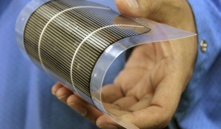
In fact, according to Twin Creek's CEO Siva Sivaram, you only need wafers that are 20 to 30 microns thick to get the charge carrier out while still getting good conversion efficiencies.
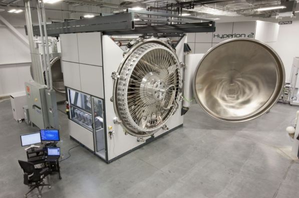
Twin Creeks allows vendors to dispense with saws, furnaces, and cell finishing equipment from the likes of Applied Materials HCT and Meyer Burger as well as slurry and thick wafers. Twin Creeks replaces that production chain with a beast of an ion implant machine (see picture below).
Ion Implantation
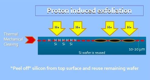
Twin Creek's process is known as PIE, for Proton-Induced Exfoliation. A hydrogen ion or proton is accelerated to 1.2 million electron-volts and shot into a crystal material -- in this case, silicon -- where it settles at a finite depth. The hydrogen ions line up at that finite depth, where they are then heated, resulting in a wafer that cleaves right off the substrate along the crystalline plane.
The proton energy determines how deep the protons go and therefore sets the thickness of the wafer.
An ion implanter is a big piece of equipment emitting protons and must be shielded for safety. Other firms performing this process have told GTM that surface roughness is better than sawn wafers, and some use an etch-and-anneal step to preserve lifetime once the wafers are cleaved.
The ion implant process produces a wafer which uses a tenth of the material, and 20-micron wafers don't crack, according to the Twin Creeks CEO who said, "At 20 microns, silicon is completely flexible."
The firm can provide a reference process for handling the unusually thin wafers. Each machine can produce 1.5 million wafers per year. That means a firm with hundred of megawatts of c-Si capacity would have to buy scores of these multi-million-dollar machines if electing to make this disruptive shift.
Twin Creek's CEO Siva Sivaram told GTM, "We are a capital equipment company and will remain a capital equipment company. San Jose is where we integrate, Boston is where the equipment is designed and built, and Mississippi is where we demo the process on a 25-megawatt cell line. There has been no marketing and there is one sales guy. We are talking now because we have a product ready to ship along with 20 issued patents and a pile on the way."
Other firms in the thin silicon business:
Ampulse claims that the firm’s "c-Si thin-film technology takes advantage of HW-CVD techniques to directly deposit a very thin layer of c-Si onto a uniquely textured and flexible metal substrate."
As reported by Ed Gunther, AstroWatt has developed a semiconductor-on-metal technology for creating thin silicon wafers. Gunther reports, "After partial processing, a monocrystalline silicon wafer is attached to an inexpensive, flexible 50-um metal foil also acting as the solar cell’s rear contact. Next, the foil, along with about 25 um of silicon, is exfoliated using a cleaving process." By reusing a 600-um wafer for multiple exfoliations, AstroWatt claims “up to 4X reduction in substrate cost” is possible, and the metal substrate is crucial for wafer handling in existing equipment." AstroWatt also stated the theoretical peak silicon solar cell efficiency can be achieved with a 25-um silicon wafer thickness.
Bandgap Engineering has developed tunable methods for nano-structuring silicon. The firm claims that the absorption of nano-silicon is enhanced by up to several orders of magnitude over bare silicon over a wide range of wavelengths. This enables nano-silicon to absorb the light in the first four microns versus the top 50 to 100 microns that bulk silicon needs to absorb most of the light. This could impact cell efficiency and direct manufacturing cost -- and make for much thinner wafers.
Crystal Solar uses a vapor deposition process for making thin crystalline silicon wafers. The firm has made wafers measuring 50 microns thick in its labs and hopes to get down to 20 microns.
1366 Technologies has a "direct wafer" technology whereby molten silicon is directly converted into wafers, which can then be processed into thin solar cells.
Silicon Genesis, known as SiGen, is also pursuing an implant-and-cleave process for wafers with thicknesses down to 20 microns.
A Disruptive Process
Backing an equipment vendor is an unorthodox approach to solar startup technology and solar venture capital in the current solar era. But certainly the billions of VC sunk into building module companies hasn't worked out very well (see Solyndra, Nanosolar, etc.) -- so equipment could be a better avenue to success.
Twin Creeks is bringing a large piece of new disruptive equipment to the current established c-Si solar manufacturing flow. If the firm can show a cost and performance benefit, there is a chance for adoption. However, capital equipment like this has a very long sales cycle and a limited number of customers.
Twin Creeks offers a disruptive change in the way solar module manufacturers make wafers and cells and threatens the way things have been typically been done. But that's what entrepreneurs do, and that's what venture capital is supposed to do. And this is an audacious and potentially disruptive bet by some brave entrepreneurs and investors. The solar industry could use the disruption.
Twin Creeks has raised more than $80 million from Crosslink Capital, Benchmark Capital, Artis, and DAG Ventures.


 41
41
 15
15
 9
9