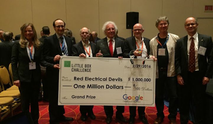
Google’s Little Box Challenge, the 19-month quest to give away $1 million to the company that can pack the most power density per square inch into a solar inverter, announced its grand prize and runners-up last week. And if the test results from the contest are any guide, winner CE+T Power has more than met Google’s big -- or, shall we say, small -- expectations.
The Belgian company’s Red Electrical Devils, named after the country's national soccer team, manage to pack 142.9 watts per square inch into a box 14 cubic inches in size. That’s nearly three times Google's minimum 50-watts-per-square-inch power density requirement, and about 10 times as power-dense as today’s commercially available models, Google said in a blog post at last week’s ARPA-E Innovation Summit outside Washington D.C.
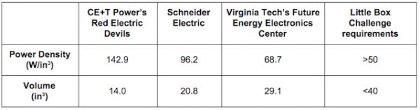
CE+T used a combination of gallium nitride (GaN) semiconductors, soft-switching techniques, and thermal management innovations to keep its 2-kilowatt inverters delivering power efficiently over 100 hours of testing at the Energy Department’s National Renewable Energy Laboratory (NREL). So did honorable-mention-winning inverters from Schneider Electric and a team from Virginia Polytechnic Institute’s Future Energy Electronics Center. Both beat Google’s power density and size thresholds handily, as this chart indicates.
If nothing else, these kinds of figures help show the promise of the next generation of wide-bandgap semiconductors such as gallium arsenide (GaN) and silicon carbide (SiC). Backed by hundreds of millions of dollars in venture capital and DOE grant funding, companies such as CE+T partner GaN Systems, Infineon-acquired International Rectifier, and Google Ventures-backed Transphorm are building transistors out of these materials, which can operate more efficiently than silicon, although at higher cost, at least today.
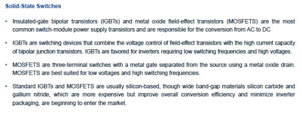
That could help shrink and cool the insulated-gate bipolar transistors (IGBTs) and metal oxide field-effect transistors (MOSFETs) that are used in today’s solar inverters. CE+T described the benefits and challenges of GaN-based inverters in its technical approach document:
GaN transistors have many very interesting electrical characteristics (low Rds_on, low Qgate and Cds, ultra low Qrr); these create technological advantages over current MOSFET and IGBT devices (small size and low production costs). Unfortunately, they also have serious drawbacks due to their very fast switching characteristics: they are challenging to drive and require sensitive electromagnetic noise management. Another pitfall is the high voltage drop due to the reverse current when the GaN is turned off.
CE+T manages these problems through the use of a “five legs topology” to reduce energy transfer within the inverter, as well as fine-tuned control via “soft switching operation of all GaN devices while minimizing reverse currents.” To reduce waste heat, “cooling is provided by the air flow of the fan and by use of an aluminum oxide foil placed in the middle of the ferrite to create the requested air gap plus a thermal drain.”
Virginia Tech’s technical documents cited wide-bandgap semiconductors, “like Transphorm’s TPH3002LD and Cree’s C3D1P7060Q employed in the DC/DC stage and GaN Systems’ GS66516T in the DC/AC stage,” noting that they allow for “higher power density, greater efficiency, and faster switching than conventional silicon devices.”
Silicon carbide (SiC) transistors, such as those provided to Little Box challengers by ST Micro, are another wide-bandgap material with promise to pack much more efficient power conversion technologies inside smaller packages.
Schneider Electric’s technical document notes that, after looking at both GaN and SiC components, “the final choice was to use SiC MOSFETs with TO247 package, which proved to be best in terms of component ruggedness, thermal management, gate driving and EM interference.”
GaN and SiC devices are “certainly part of the roadmap for more efficient, less costly solar inverters,” according to MJ Shiao, solar research director for GTM Research. Commercial products are being developed, he said, citing the work going on between Transphorm and partners like Yaskawa and Enphase and Tata to build GaN-based solar inverters.
As for building a commercial-scale business on these novel semiconductors, however, “The issue, as always, is scale, track record, cost and diversity of suppliers,” Shiao said. Most of today’s inverters are already highly efficient, losing only a few percentage points of power in DC-to-AC conversion.
Google got more than 2,000 entrants after it launched the contest in mid-2014, and picked a list of 18 finalists in October, including universities, research organizations and a host of startups. All finalists’ technical approach documents will be posted on the Little Box Challenge website through the end of 2017, Google said.
Google has been quietly working on power electronics development outside the Little Box Challenge. Last week’s announcement didn’t say exactly what the company intends to do next with the technologies it’s unearthed and rewarded, besides noting, “We hope this helps advance the state of the art and innovation in kW-scale inverters.”
Here’s a GTM Research breakdown of the power electronics inside inverters, and how GaN and SiC devices could fit into the current market landscape.


 41
41
 15
15
 9
9