As the computing revolution marches forward, energy efficiency is becoming increasingly important.
The explosion of computing over the last 20 years has created many societal benefits -- but its energy and environmental footprint has correspondingly grown as well.
The evolution toward cloud computing, “always-on” connectivity, and immersive experiences, including virtual and augmented reality, are adding demands for efficient computing performance. There are projections that information and communications technologies, including computers and cell phones, will consume 14 percent of worldwide electricity by 2020.
The result of all these factors is a strong market pull for technologies that improve processor performance while also reducing energy use. Energy efficiency is typically defined as the combination of improving performance while maintaining or reducing energy use.
Historically, improvements in energy efficiency have largely come as a byproduct of Moore’s law -- the doubling of the number of transistors on a chip about every two years through ever-smaller circuitry. In general, more transistors on a single computer chip and less physical distance between them leads to better performance and improved energy efficiency.
However, the energy-related benefits that result from Moore’s law are slowing down, potentially threatening future advances in computing. We’ve reached a level where the miniaturization of transistors is now bumping up against physical limits. That’s because smaller transistors have thinner insulating layers, which leads to a loss of electrical current through leakage, requiring more power to offset the lost current.
As transistors are continually getting smaller, the leaking current becomes an even greater engineering challenge. This, in part, has led many to question whether Moore’s law will continue at its traditional pace.
Historically, as transistors became smaller, power efficiency improved in tandem with processor speed. Now, this steady increase in efficiency has slowed. Therefore, it’s increasingly clear that semiconductor designers will need to develop creative measures to supplement the slowing energy efficiency gains.
At AMD, we have taken on a significant goal of improving the energy efficiency of our products -- specifically, to improve the energy efficiency of our mobile processors by 25 times between 2014 and 2020. We refer to this as our 25x20 initiative. How well we and others in the industry respond to the slowing of efficiency gains may have profound implications for the global economy and the environment as society increasingly relies on digital technologies.
But if the historical method -- that is, manufacturing technologies for greater transistor density -- no longer has the same impact as before, what can the industry do as an offset in order to make future energy efficiency gains? At the processor level, the answers for now are new processor architectures, power efficient technologies, and power management techniques.
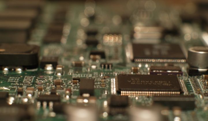
For decades, the central processing unit (CPU) of a computer has been designed to run general programming tasks. These processors excel at running computing instructions serially -- if condition A exists, then perform B, then C, etc., one step after the other -- and they increasingly use a variety of complex techniques and algorithms in order to improve speed.
By contrast, graphical processing units (GPUs) are specialized accelerators originally designed for painting millions of pixels simultaneously across a screen. GPUs do this by performing calculations in parallel using a comparatively simple architecture. CPUs and GPUs have traditionally run as separate processors, on separate chips or integrated circuit boards within a PC, gaming console, tablet, smartphone, and most recently, in some servers and supercomputers.
Today, the CPU and GPU are increasingly being integrated into a single entity. AMD refers to this combination as an accelerated processing unit (APU).
While a significant step in the right direction, work remains to bring the two processor types into a harmonious and heterogeneous alignment that can improve performance and minimize energy consumption. This has led to an emerging industry standard, known as the heterogeneous systems architecture (HSA).
The net effect of HSA is to allow the CPU and GPU to operate as peers within the APU, dramatically reducing the complexity and overhead. Many workloads, such as natural human interfaces and pattern recognition, benefit from the parallel execution of the GPU and execute many times more efficiently when both GPU and CPU are used cooperatively.
These capabilities are important for many applications, including voice recognition, data security, medical imaging, genome sequencing, autonomous driving, and supercomputer applications focused on primary scientific research. In addition to facilitating next-generation use cases, this practical merging of the two processor types can result in a dramatic improvement in performance and energy efficiency. New processor chips employing HSA are just now entering the market with AMD’s latest APUs, paving the way for new applications and capabilities.
Changing computer workloads can also affect the power use of the processors. Most computers run at peak output only a small fraction of the time, often as little as 1 percent.
Consequently, most computing today is typically characterized by idle time -- those periods between keystrokes or frames of a video, or after a web page loads. Energy-efficient technologies optimized for reducing energy use while idle and optimized for “typical-use” scenarios enable further energy-efficiency gains.
For example, when there are peak computing demands, such as with video rendering, processors require more electricity, a requirement which then diminishes when the task is complete. The sudden changes cause significant fluctuations in the chip’s power supply. Microprocessor designers typically supply an excess amount of power to ensure the processor always has a sufficient amount to meet peak demand, but this practice is costly in terms of energy.
Rapidly adjusting the voltage to meet changing application can offer an opportunity to eliminate wasted power. AMD’s latest processors include these voltage adaptive capabilities and functions in both the CPU and the GPU, helping to cut power by 10 percent to 20 percent.
Beyond architecture and power-efficient silicon, power management techniques can drive further energy-efficiency gains. One example is through very fine-grained monitoring and management of power, temperature, and activity across the APU. This allows a processor to dynamically allocate power based on application need. As performance is increased, tasks are completed more rapidly and therefore the device can spend more time in idle modes -- resulting in a “virtuous cycle” of higher performance and lower power that synergistically improves efficiency.
Furthermore, new approaches in packaging integration are delivering significant miniaturization and a reduction of power. AMD is the first in the industry with announced plans to deploy high bandwidth memory (HBM) in GPUs and targeting significant reductions in power. The HBM graphics memory is a 3-D vertical stack connected to the GPU over a silicon carrier (2.5D packaging). The resulting silicon-to-silicon connection consumes more than three times less power than DDR5 memory.
In summary, no one can say just when or if Moore’s law will cease to be applicable; however, there’s no doubt that associated energy-efficiency gains have slowed substantially.
At the same time, the energy consumption incurred by society’s growing use of computing devices is increasing. This necessitates clever engineering to overcome the physical limits of ever-smaller transistors in order to continue to grow the amazing enhancements computing has brought to so many. In the future, the bulk of the energy-efficiency gains will stem from architecture, new circuit design and power-management techniques.
***
Mark Papermaster is chief technology officer and senior vice president at AMD, responsible for corporate technical direction, as well as AMD’s intellectual property and system-on-chip product research and development.


 41
41
 15
15
 9
9