About a year ago, Sydney, Australia-based BT Imaging (BTi) received $3.8 million in funding from Applied Ventures, the VC arm of Applied Materials (NASDAQ: AMAT), along with investors Allen & Buckeridge and Uniseed.
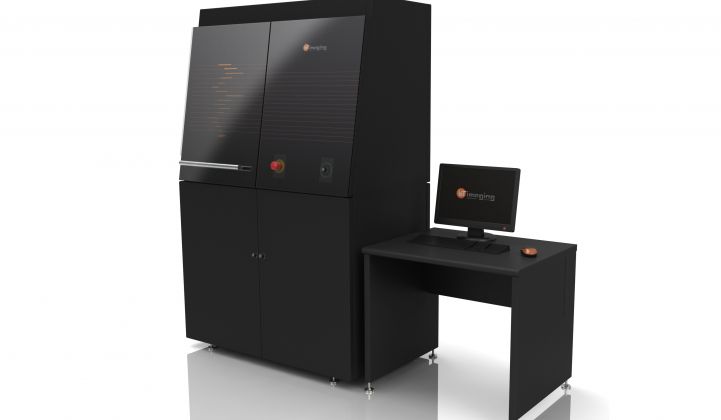
The firm is now shipping a production tool into the PV manufacturing ecosystem.
BTi improves solar cell efficiency and manufacturing yields by applying photoluminescence imaging to the manufacturing and testing of silicon wafers and solar cells. BTi claims to have invented the concept of applying photoluminescence imaging to silicon.
BTi’s luminescence imaging systems are used for research, process development, production manufacturing inspection, and quality control of silicon blocks, wafers, and PV cells. Originally developed at the University of New South Wales, BT Imaging's photoluminescence technology allows real-time electronic inspection of every wafer or solar cell processed through a manufacturing line.
The company started out building R&D and lab equipment for testing crystalline silicon solar cells. After shipping a number of R&D tools, the feedback was that customers needed in-line tools. "In-situ monitoring capability is truly a gaping hole in PV manufacturing," said a colleague at an emerging PV cell firm.
I spoke with Wayne McMillan, the VP of Sales and Marketing. He spoke of the improvements that BTi enables in efficiency and yield from silicon blocks all the the way to the module level. McMillan claims that their tools are much faster and provide much better resolution than existing solutions. The firm will soon be introducing tools that can inspect 3,600 wafers per hour.
The photoluminescence technology used by BTi "uniformly illuminates the entire sample with near IR laser light and generates electron and hole pairs." As those carriers recombine, the light is collected with a special CCD-type camera. Anything that looks dark on the image is electrically poor.
The customer is looking for flaws and defects, such as crystal dislocation defects and impurities. High recombination equals low carrier lifetime equals areas of low efficiency, according to company representatives. Dislocations can reduce absolute cell efficiency by 1 percent. The customer can then recycle flawed blocks and wafers prior to the next processing steps.
Their R&D tool is sold to ingot, wafer, cell and module makers.
But it's not the imaging that the customers really need -- what's more important is what you do with the data and how it is classified. According to the VP, "In production, the customer doesn't want images -- they want data and analysis." So software and algorithms are as important as the imaging itself.
BT Imaging systems can be used to predict cell performance, material quality control, process and material faults, and for process control and debugging. The company’s inspection and QC control systems are used by wafer and cell manufacturers in Europe, Australia, Taiwan, China, and Japan.
The value of the tool is clear. Manufacturers are pushing efficiency boundaries with new manufacturing techniques such as back contacts or selective emitters. According to McMillan, "When you're spending that extra money, you want to start with a higher efficiency wafer." He adds, "We see a case for sorting the wafers for high efficiency lines," and if you have a low performance wafer -- you can perform a gettering step and "suck out impurities" with high temperature processing and dopant strips.
The bottom line, according to McMillan, is that "the tool helps improve efficiency and yield."
Firms like AccuStrata, Laytec, and Brightview Systems are also looking at PV cell metrology and process control, although mostly in thin film.


 41
41
 15
15
 9
9