
Ions are in the air this month.
Last week, Twin Creeks made a splash with its ion-implant technology, aiming to reduce silicon material usage in solar panels and thus reduce cost. We covered the details here.
That unstealthing must have caught SiGen a bit off-guard, as that company appears to be hustling to let the world know that it is working on this technology too. SiGen has sent a few warnings about intellectual property ownership, as well.
We've covered SiGen and its thin silicon brethren in the past.
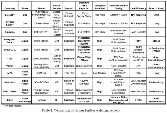
Current silicon wafer thickness is in the 150-micron range. Traditionally, wafers are freed from blocks of silicon using wire saws in a process that is messy, complex and reaching its technological limits. The wire saws use silicon carbide as an abrasive in the slurry and it's difficult to reclaim the lost materials from the resulting sawdust-SiC mix. There is a cost to the lost materials, as well as the spent wires themselves. As manufacturers push the limit of wafer thickness, they are resorting to even more expensive methods, such as diamond wire saws.
It's an obvious weak link and cost target in the solar value chain. Manufacturers spend a great deal of time and energy to fabricate blocks of polysilicon, only to see up to half of that hard-earned material turned into sawdust in the wafer production step. Thin silicon with dimensions of 20 microns could be a disruptive change in the solar manufacturing story.
The idea with kerfless silicon is to eliminate saws, furnaces, and cell finishing equipment from the likes of Applied Materials HCT and Meyer Burger as well as slurry and thick wafers. Both SiGen and Twin Creeks intend to replace that production chain with a beast of an ion implant machine. The challenging goal is for the new process to fit seamlessly into solar vendor production flow with little impact on wafer handling, interconnection, packaging, and reliability. Those crucial issues have not been proven at full production, although Twin Creeks has a 25-megawatt line in Mississippi, as well as a reference process for module production.
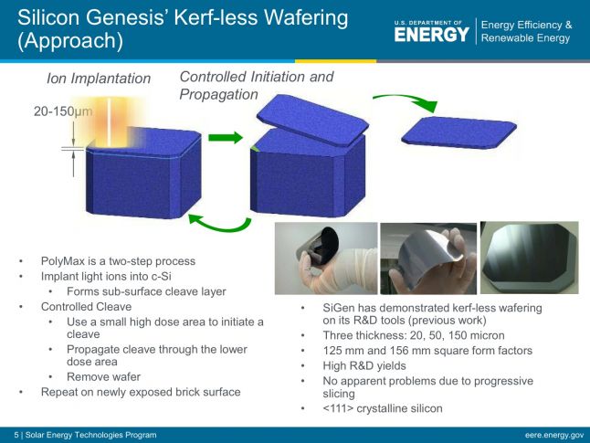
Ion implant technology accelerates protons to 1.2 million electron-volts and shoots them into a crystal material -- in this case, silicon -- where they settle at a finite depth. The hydrogen ions line up at that finite depth, where they are then heated, resulting in a wafer that cleaves right off the substrate along the crystalline plane. The proton energy determines how deep the protons go and therefore sets the thickness of the wafer.
SiGen claims that its thin wafers are "free-standing," while those of Twin Creeks must be bonded to a metal substrate.
SiGen has also made some not-so-subtle patent intimations in a press release today, saying, "We are also closely following recent announcements by Twin Creeks Technologies of a process similar to our beam-induced wafering. [...] As the pioneers of beam-induced wafering and assuming it is not utilizing any of our technology embodied in our 100+ U.S. patent portfolio which we are monitoring," adding, "The fact that Twin Creeks Technologies was founded by a venture capital firm shortly after it evaluated SiGen’s beam-induced wafering business plan and technology, including our prototype 2 million electron volt implanter is of concern.”
The CEO of Twin Creeks had no comment on this issue.
SiGen, like Twin Creeks, builds an enormous piece of production equipment. Neither firm is in the solar module manufacturing business.
SiGen is just one of many startups pursuing novel ways of transforming blocks of silicon into thin solar wafers in a less wasteful and less expensive fashion.
Other firms in the thin silicon business include:
Ampulse claims that the firm’s "c-Si thin film technology takes advantage of HW-CVD techniques to directly deposit a very thin layer of c-Si onto a uniquely textured and flexible metal substrate."
AstroWatt, as reported by Ed Gunther, has developed a semiconductor-on-metal technology for creating thin silicon wafers. Gunther reports, "After partial processing, a monocrystalline silicon wafer is attached to an inexpensive, flexible 50-um metal foil also acting as the solar cell’s rear contact. Next, the foil, along with about 25 um of silicon, is exfoliated using a cleaving process. By reusing a 600-um wafer for multiple exfoliations, AstroWatt claims “up to 4X (four times) reduction in substrate cost” is possible, and the metal substrate is crucial for wafer handling in existing equipment. AstroWatt also stated the theoretical peak silicon solar cell efficiency can be achieved with a 25-um silicon wafer thickness.
Bandgap Engineering has developed tunable methods for nano-structuring silicon. The firm claims that the absorption of nano-silicon is enhanced by up to several orders of magnitude over bare silicon over a wide range of wavelengths. This enables nano-silicon to absorb the light in the first four microns versus the top 50 to 100 microns that bulk silicon needs to absorb most of the light. This could impact cell efficiency and direct manufacturing cost -- and make for much thinner wafers.
Crystal Solar uses a vapor deposition process for making thin crystalline silicon wafers. The firm has made wafers measuring 50 microns thick in its labs and hopes to get down to 20 microns.
1366 Technologies has a "direct wafer" technology whereby molten silicon is directly converted into wafers, which can then be processed into thin solar cells.
Here's SiGen's take on the competitors:
Developing a new wafer technology and integrating it into an existing process chain remains an enormous challenge.


 41
41
 15
15
 9
9