Earlier this year, 1366 Technologies of Bedford, Mass., a startup with VC funding and a DOE loan guarantee, opened a $6 million, 25-megawatt wafer fabrication facility.
Things must be going well because the company just landed an additional $15 million that is slated to be used to build a 250-megawatt factory, with construction set to start in 2014.
Investors in this round include Tokuyama Corporation, North Bridge Venture Partners, Polaris Venture Partners, VantagePoint Capital Partners and Energy Technology Ventures (a JV involving General Electric, NRG Energy and ConocoPhillips). 1366 has raised a total of $64 million in venture funding from additional investors including Hanwha Chemical (Hanwha is also a potential customer) and Ventizz Capital. In addition, 1366 has won several million dollars in DOE grants, as well as a $150 million loan guarantee offer from the DOE's 1705 program, but the loan money is to be drawn down for the buildout of a larger, gigawatt-scale factory.
Frank van Mierlo, the CEO of 1366, said in a statement, "We’ve taken a very deliberate route to high-volume production. In the process, we’ve built a stable, capital-efficient business during the most challenging of times.”
“1366 Technologies has the enormous benefit of being a ‘drop-in’ replacement for 60 percent of the photovoltaics market,” said Hidenori Okamoto, Managing Executive Officer of Tokuyama Corporation.
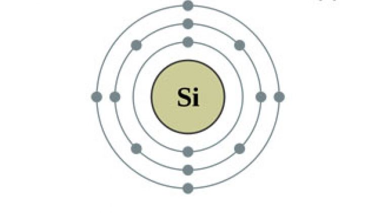
The company's technology falls in the "kerfless wafer" category, a technology that was of special interest to former DOE head Steven Chu. 1366's technology creates wafers directly from molten silicon, though the firm has not divulged specific details about its process.
The aim is to disrupt the traditional way that silicon-based photovoltaic wafers are fabricated. The company claims that it has demonstrated "manufacturing rates of more than 1,200 wafers per furnace per day -- with a goal of more than 3,500 wafers per day for each furnace -- on par with standard ingot casting furnaces."
As van Mierlo told GTM in an earlier interview, "For the last 50 years, we've been melting silicon, creating ingots and blocks, and cutting the blocks with wire saws to create wafers," noting that the incumbent process uses eighteen different machines and goes through "a lot of consumables," adding, "Half of the silicon is wasted."
"Our process has none of these consumables," said the CEO, noting that 1366 uses one-quarter of the factory real estate and doesn't waste silicon in its "semi-continuous process."
The end product is a textured wafer in a standard 156-by-156-by-0.2 millimeter size. According to the CEO, "It goes into any standard cell line." The process has yielded efficiencies of 17.2 percent in customer trials, according to the company.
Other companies in the kerfless silicon sector include Solexel, Scifiniti, and Crystal Solar.
Van Mierlo has also claimed, "Our production costs are significantly lower than the variable cost of the legacy solution. [...] We will have fully loaded production costs of less than 10 cents per watt."
Since mid-2010, the DOE has made conditional commitments for eighteen loan guarantees in solar to fourteen different companies for a total of $15.585 billion. The bottom line is that the program will end up making money, not losing it. But it's fair to say that loans for solar manufacturing have been less successful than loans for solar generation. The manufacturing firms given loans include SoloPower, Abound Solar, and the now-defunct Solyndra.
Van Mierlo has likened the 1366 innovation in silicon to the Bessemer process innovation at U.S. Steel or the use of float glass at Pilkington.
He said, "New manufacturing processes change the way things get done," adding, "Our prospects are as good as U.S. Steel's were two centuries ago."


 41
41
 15
15
 9
9