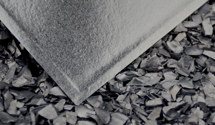
1366 Technologies, a Massachusetts firm working to slash the cost of silicon-based photovoltaics, has developed a "3-D" wafer that further reduces the amount of silicon needed to produce the building block of a solar cell.
The product was developed to address industry-wide limitations in wafer thickness -- and thus limitations in cost reduction.
Over the years, producers have steadily slimmed down wafers with better sawing techniques, bringing the industry standard to 180-200 microns in thickness. But wafers thinner than 180 microns are much more vulnerable to breaking when turned into cells. So 1366 engineers looked at how to strip more silicon out of the wafer, while strengthening potential stress points.
The result: a wafer with a border that is 180-200 microns thick, and a middle section that is 100-120 microns thick. The product further reduces silicon consumption and gets 1366 Technologies closer to its goal of cutting wafer costs by half. (Wafers make up about 40 percent of the total cost of a PV module.)
By abandoning the traditional process used to grow ingots and cut wafers, 1366 Technologies can be more creative with wafer design.
In traditional wafer production, silicon is melted into blocks that are then sliced by wire saws. The growth and sawing process requires more than a dozen machines -- and it wastes a lot of time, energy and silicon.
"It's pretty archaic," said Frank van Mierlo, the CEO of 1366 Technologies in an interview at the company's offices. "There's so much waste in the wafer-making process."
Instead of forming big blocks of silicon that are sawed into wafers, 1366 melts silicon in a bath-like furnace. Wafers are molded one at a time at the top layer of the molten silicon bath, and then removed without sawing of any kind. According to van Mierlo, the company can produce double the wafers from the same amount of silicon compared to the conventional process.
"We're also cutting the energy to make a wafer by a factor of three," he said. "There's very little waste."
The simplified process allows 1366 to make modifications to each side of the wafer -- which is how it can make a 3-D product with varying levels of thickness.
The 3-D wafer is about one year behind 1366's current commercial product. When fully validated by customers, it can simply be added to existing wafer production lines -- part of 1366 Technologies' mission since its inception.
"We’re always looking at something that fits into the existing supply chain," said Adam Lorenz, the company's vice president of product development.
While 1366 has pivoted slightly over the years (it started with a focus on honeycomb-textured wafers), it has always stuck by its mission of building equipment that can be easily integrated into manufacturing operations. After all, what good is cutting wafer costs by half if you have to rebuild an entire production line around it?
When 1366 Technologies was founded in 2008 with the goal of slashing the cost of manufacturing silicon solar wafers, the industry was undergoing a major transition. Many believed that traditional crystalline silicon was approaching cost and performance limitations, and that thin film, or technologies like perovskites or quantum dots, would soon take over.
Many billions of dollars were invested into factories by venture capitalists who believed in that thesis -- and many billions of dollars were lost. Eight years later, multicrystalline solar cells make up nearly three-quarters of the global market, while thin film represents just 6 percent.
"I’ve never doubted silicon," said van Mierlo. "We really believed in it. The learning curve had been holding steady for 45 years -- it’s a pretty predicable line. Why would that stop?"
Over the years, 1366 Technologies has quietly built three generations of equipment for making silicon wafers at its Bedford, Massachusetts facility, with each generation producing better and cheaper products.
Unlike many other manufacturers in solar that have experienced spectacular growth -- and, in some cases, spectacular downfalls -- 1366 grew cautiously in an effort to fully validate its wafer production process and partner with leading cell producers. It is now in a position to start scaling quickly, said van Mierlo.
The new 3-D wafer design caps a strong year for 1366 Technologies. In recent months, the company inked a 700-megawatt supply agreement with Hanwha Q-Cells, raised $25 million from Hanwha and Wacker Chemie, achieved a 19.1-percent-efficient cell using its wafers in partnership with Hanwha Q-Cells, and announced plans to build a 250-megawatt wafer production facility in New York.
The company also hit another important milestone. On the day of the interview, 1366 Technologies sent out its largest shipment to date -- 100,000 wafers.
"Solar will continue to get cheaper faster than people predict. We still have more room to better engineer these technologies," said van Mierlo.
Is the future of solar in silicon? Listen to our interview with Dick Swanson, the founder of SunPower, about how manufacturers were able to drop the cost of producing silicon-based solar panels 200-fold.


